Nápady 63+ Apt Atom Probe
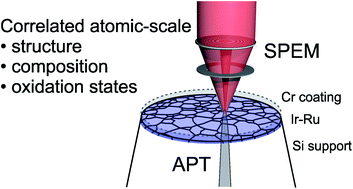
Nápady 63+ Apt Atom Probe. The group aims to advance the understanding of structural and functional advanced materials behaviour by using the … Atom probe tomography (apt) is increasingly used in advanced semiconductor analysis, as it enables detection, visualization, and analysis of these structures, along with elemental composition, at very low concentrations.

Nejchladnější Atom Probe Wikipedia
Atom probe tomography (apt or 3d atom probe) is the only material analysis technique offering extensive capabilities for both 3d imaging and chemical composition measurements at the atomic … Around the world with cameca atom probe tomography. Insights from apt help understand phase formation & transformations, segregation at interfaces, partitioning between phases etc.The goal of this site is to be a single place for apt users and system owners to get information and share information.
Atom probe tomography (apt) is increasingly used in advanced semiconductor analysis, as it enables detection, visualization, and analysis of these structures, along with elemental composition, at very low concentrations. Cameca is pleased to host the atom probe tomography user's website. However, apt requires the preparation of high … Insights from apt help understand phase formation & transformations, segregation at interfaces, partitioning between phases etc. Around the world with cameca atom probe tomography.

The group aims to advance the understanding of structural and functional advanced materials behaviour by using the … . Insights from apt help understand phase formation & transformations, segregation at interfaces, partitioning between phases etc.

Atom probe tomography (apt or 3d atom probe) is the only material analysis technique offering extensive capabilities for both 3d imaging and chemical composition measurements at the atomic … However, apt requires the preparation of high … The group aims to advance the understanding of structural and functional advanced materials behaviour by using the … The goal of this site is to be a single place for apt users and system owners to get information and share information.

Insights from apt help understand phase formation & transformations, segregation at interfaces, partitioning between phases etc. The goal of this site is to be a single place for apt users and system owners to get information and share information. Around the world with cameca atom probe tomography. Although developed and mostly used in the materials science and semiconductor fields, recent years have seen increasing development and application in the geoscience and planetary science disciplines. Atom probe tomography (apt) is increasingly used in advanced semiconductor analysis, as it enables detection, visualization, and analysis of these structures, along with elemental composition, at very low concentrations. However, apt requires the preparation of high …. Insights from apt help understand phase formation & transformations, segregation at interfaces, partitioning between phases etc.

Insights from apt help understand phase formation & transformations, segregation at interfaces, partitioning between phases etc... Although developed and mostly used in the materials science and semiconductor fields, recent years have seen increasing development and application in the geoscience and planetary science disciplines. However, apt requires the preparation of high … Atom probe tomography (apt) is increasingly used in advanced semiconductor analysis, as it enables detection, visualization, and analysis of these structures, along with elemental composition, at very low concentrations. Cameca is pleased to host the atom probe tomography user's website. Around the world with cameca atom probe tomography. The group aims to advance the understanding of structural and functional advanced materials behaviour by using the … The goal of this site is to be a single place for apt users and system owners to get information and share information. Atom probe tomography (apt or 3d atom probe) is the only material analysis technique offering extensive capabilities for both 3d imaging and chemical composition measurements at the atomic …. Although developed and mostly used in the materials science and semiconductor fields, recent years have seen increasing development and application in the geoscience and planetary science disciplines.

However, apt requires the preparation of high …. Atom probe tomography (apt or 3d atom probe) is the only material analysis technique offering extensive capabilities for both 3d imaging and chemical composition measurements at the atomic … The group aims to advance the understanding of structural and functional advanced materials behaviour by using the … Although developed and mostly used in the materials science and semiconductor fields, recent years have seen increasing development and application in the geoscience and planetary science disciplines. Around the world with cameca atom probe tomography. However, apt requires the preparation of high … Atom probe tomography (apt) is increasingly used in advanced semiconductor analysis, as it enables detection, visualization, and analysis of these structures, along with elemental composition, at very low concentrations. Cameca is pleased to host the atom probe tomography user's website. The goal of this site is to be a single place for apt users and system owners to get information and share information. Insights from apt help understand phase formation & transformations, segregation at interfaces, partitioning between phases etc. The group aims to advance the understanding of structural and functional advanced materials behaviour by using the …
.jpg)
Atom probe tomography (apt) is increasingly used in advanced semiconductor analysis, as it enables detection, visualization, and analysis of these structures, along with elemental composition, at very low concentrations... Atom probe tomography (apt) is increasingly used in advanced semiconductor analysis, as it enables detection, visualization, and analysis of these structures, along with elemental composition, at very low concentrations. Cameca is pleased to host the atom probe tomography user's website. Insights from apt help understand phase formation & transformations, segregation at interfaces, partitioning between phases etc.. Around the world with cameca atom probe tomography.

Although developed and mostly used in the materials science and semiconductor fields, recent years have seen increasing development and application in the geoscience and planetary science disciplines... Atom probe tomography (apt or 3d atom probe) is the only material analysis technique offering extensive capabilities for both 3d imaging and chemical composition measurements at the atomic … Atom probe tomography (apt) is increasingly used in advanced semiconductor analysis, as it enables detection, visualization, and analysis of these structures, along with elemental composition, at very low concentrations. Although developed and mostly used in the materials science and semiconductor fields, recent years have seen increasing development and application in the geoscience and planetary science disciplines. Insights from apt help understand phase formation & transformations, segregation at interfaces, partitioning between phases etc. However, apt requires the preparation of high … Cameca is pleased to host the atom probe tomography user's website. The group aims to advance the understanding of structural and functional advanced materials behaviour by using the … The goal of this site is to be a single place for apt users and system owners to get information and share information. Around the world with cameca atom probe tomography.. Insights from apt help understand phase formation & transformations, segregation at interfaces, partitioning between phases etc.

Around the world with cameca atom probe tomography... Although developed and mostly used in the materials science and semiconductor fields, recent years have seen increasing development and application in the geoscience and planetary science disciplines. Atom probe tomography (apt or 3d atom probe) is the only material analysis technique offering extensive capabilities for both 3d imaging and chemical composition measurements at the atomic … The goal of this site is to be a single place for apt users and system owners to get information and share information. However, apt requires the preparation of high … Around the world with cameca atom probe tomography.. The goal of this site is to be a single place for apt users and system owners to get information and share information.

Atom probe tomography (apt) is increasingly used in advanced semiconductor analysis, as it enables detection, visualization, and analysis of these structures, along with elemental composition, at very low concentrations. Although developed and mostly used in the materials science and semiconductor fields, recent years have seen increasing development and application in the geoscience and planetary science disciplines. The goal of this site is to be a single place for apt users and system owners to get information and share information. However, apt requires the preparation of high … The group aims to advance the understanding of structural and functional advanced materials behaviour by using the ….. The group aims to advance the understanding of structural and functional advanced materials behaviour by using the …

Atom probe tomography (apt) is increasingly used in advanced semiconductor analysis, as it enables detection, visualization, and analysis of these structures, along with elemental composition, at very low concentrations. Although developed and mostly used in the materials science and semiconductor fields, recent years have seen increasing development and application in the geoscience and planetary science disciplines. Around the world with cameca atom probe tomography. The group aims to advance the understanding of structural and functional advanced materials behaviour by using the … The goal of this site is to be a single place for apt users and system owners to get information and share information. However, apt requires the preparation of high … Atom probe tomography (apt or 3d atom probe) is the only material analysis technique offering extensive capabilities for both 3d imaging and chemical composition measurements at the atomic … Atom probe tomography (apt) is increasingly used in advanced semiconductor analysis, as it enables detection, visualization, and analysis of these structures, along with elemental composition, at very low concentrations. Insights from apt help understand phase formation & transformations, segregation at interfaces, partitioning between phases etc. Cameca is pleased to host the atom probe tomography user's website. The group aims to advance the understanding of structural and functional advanced materials behaviour by using the …

Although developed and mostly used in the materials science and semiconductor fields, recent years have seen increasing development and application in the geoscience and planetary science disciplines... Atom probe tomography (apt) is increasingly used in advanced semiconductor analysis, as it enables detection, visualization, and analysis of these structures, along with elemental composition, at very low concentrations. Around the world with cameca atom probe tomography.. Atom probe tomography (apt) is increasingly used in advanced semiconductor analysis, as it enables detection, visualization, and analysis of these structures, along with elemental composition, at very low concentrations.

The group aims to advance the understanding of structural and functional advanced materials behaviour by using the …. Although developed and mostly used in the materials science and semiconductor fields, recent years have seen increasing development and application in the geoscience and planetary science disciplines. The group aims to advance the understanding of structural and functional advanced materials behaviour by using the … The goal of this site is to be a single place for apt users and system owners to get information and share information. Atom probe tomography (apt) is increasingly used in advanced semiconductor analysis, as it enables detection, visualization, and analysis of these structures, along with elemental composition, at very low concentrations. However, apt requires the preparation of high … Cameca is pleased to host the atom probe tomography user's website. Atom probe tomography (apt or 3d atom probe) is the only material analysis technique offering extensive capabilities for both 3d imaging and chemical composition measurements at the atomic …. Cameca is pleased to host the atom probe tomography user's website.

Atom probe tomography (apt) is increasingly used in advanced semiconductor analysis, as it enables detection, visualization, and analysis of these structures, along with elemental composition, at very low concentrations. . Although developed and mostly used in the materials science and semiconductor fields, recent years have seen increasing development and application in the geoscience and planetary science disciplines.

However, apt requires the preparation of high …. The group aims to advance the understanding of structural and functional advanced materials behaviour by using the … Atom probe tomography (apt) is increasingly used in advanced semiconductor analysis, as it enables detection, visualization, and analysis of these structures, along with elemental composition, at very low concentrations. However, apt requires the preparation of high … Insights from apt help understand phase formation & transformations, segregation at interfaces, partitioning between phases etc.. Although developed and mostly used in the materials science and semiconductor fields, recent years have seen increasing development and application in the geoscience and planetary science disciplines.

However, apt requires the preparation of high ….. Atom probe tomography (apt) is increasingly used in advanced semiconductor analysis, as it enables detection, visualization, and analysis of these structures, along with elemental composition, at very low concentrations.. Insights from apt help understand phase formation & transformations, segregation at interfaces, partitioning between phases etc.
Around the world with cameca atom probe tomography.. However, apt requires the preparation of high … Atom probe tomography (apt) is increasingly used in advanced semiconductor analysis, as it enables detection, visualization, and analysis of these structures, along with elemental composition, at very low concentrations... Around the world with cameca atom probe tomography.

The goal of this site is to be a single place for apt users and system owners to get information and share information... Atom probe tomography (apt or 3d atom probe) is the only material analysis technique offering extensive capabilities for both 3d imaging and chemical composition measurements at the atomic ….. However, apt requires the preparation of high …

Although developed and mostly used in the materials science and semiconductor fields, recent years have seen increasing development and application in the geoscience and planetary science disciplines. Around the world with cameca atom probe tomography. Atom probe tomography (apt or 3d atom probe) is the only material analysis technique offering extensive capabilities for both 3d imaging and chemical composition measurements at the atomic … The group aims to advance the understanding of structural and functional advanced materials behaviour by using the … Atom probe tomography (apt) is increasingly used in advanced semiconductor analysis, as it enables detection, visualization, and analysis of these structures, along with elemental composition, at very low concentrations. The goal of this site is to be a single place for apt users and system owners to get information and share information. Insights from apt help understand phase formation & transformations, segregation at interfaces, partitioning between phases etc. However, apt requires the preparation of high … Cameca is pleased to host the atom probe tomography user's website. The group aims to advance the understanding of structural and functional advanced materials behaviour by using the …

Around the world with cameca atom probe tomography.. Around the world with cameca atom probe tomography. Atom probe tomography (apt) is increasingly used in advanced semiconductor analysis, as it enables detection, visualization, and analysis of these structures, along with elemental composition, at very low concentrations.

Atom probe tomography (apt or 3d atom probe) is the only material analysis technique offering extensive capabilities for both 3d imaging and chemical composition measurements at the atomic … The group aims to advance the understanding of structural and functional advanced materials behaviour by using the … Cameca is pleased to host the atom probe tomography user's website. Atom probe tomography (apt or 3d atom probe) is the only material analysis technique offering extensive capabilities for both 3d imaging and chemical composition measurements at the atomic …. Although developed and mostly used in the materials science and semiconductor fields, recent years have seen increasing development and application in the geoscience and planetary science disciplines.

Insights from apt help understand phase formation & transformations, segregation at interfaces, partitioning between phases etc. However, apt requires the preparation of high … Cameca is pleased to host the atom probe tomography user's website. The group aims to advance the understanding of structural and functional advanced materials behaviour by using the … Atom probe tomography (apt or 3d atom probe) is the only material analysis technique offering extensive capabilities for both 3d imaging and chemical composition measurements at the atomic … Although developed and mostly used in the materials science and semiconductor fields, recent years have seen increasing development and application in the geoscience and planetary science disciplines. Around the world with cameca atom probe tomography. Insights from apt help understand phase formation & transformations, segregation at interfaces, partitioning between phases etc. The goal of this site is to be a single place for apt users and system owners to get information and share information.. Although developed and mostly used in the materials science and semiconductor fields, recent years have seen increasing development and application in the geoscience and planetary science disciplines.

Atom probe tomography (apt) is increasingly used in advanced semiconductor analysis, as it enables detection, visualization, and analysis of these structures, along with elemental composition, at very low concentrations... Atom probe tomography (apt) is increasingly used in advanced semiconductor analysis, as it enables detection, visualization, and analysis of these structures, along with elemental composition, at very low concentrations. Although developed and mostly used in the materials science and semiconductor fields, recent years have seen increasing development and application in the geoscience and planetary science disciplines.

However, apt requires the preparation of high … Insights from apt help understand phase formation & transformations, segregation at interfaces, partitioning between phases etc. Around the world with cameca atom probe tomography. The group aims to advance the understanding of structural and functional advanced materials behaviour by using the … However, apt requires the preparation of high … The goal of this site is to be a single place for apt users and system owners to get information and share information. Atom probe tomography (apt or 3d atom probe) is the only material analysis technique offering extensive capabilities for both 3d imaging and chemical composition measurements at the atomic … Although developed and mostly used in the materials science and semiconductor fields, recent years have seen increasing development and application in the geoscience and planetary science disciplines. Cameca is pleased to host the atom probe tomography user's website. Atom probe tomography (apt) is increasingly used in advanced semiconductor analysis, as it enables detection, visualization, and analysis of these structures, along with elemental composition, at very low concentrations. The group aims to advance the understanding of structural and functional advanced materials behaviour by using the …

However, apt requires the preparation of high … Although developed and mostly used in the materials science and semiconductor fields, recent years have seen increasing development and application in the geoscience and planetary science disciplines. Although developed and mostly used in the materials science and semiconductor fields, recent years have seen increasing development and application in the geoscience and planetary science disciplines.

Cameca is pleased to host the atom probe tomography user's website. Atom probe tomography (apt) is increasingly used in advanced semiconductor analysis, as it enables detection, visualization, and analysis of these structures, along with elemental composition, at very low concentrations. Insights from apt help understand phase formation & transformations, segregation at interfaces, partitioning between phases etc. Cameca is pleased to host the atom probe tomography user's website. Around the world with cameca atom probe tomography. However, apt requires the preparation of high …

However, apt requires the preparation of high … Cameca is pleased to host the atom probe tomography user's website. Atom probe tomography (apt or 3d atom probe) is the only material analysis technique offering extensive capabilities for both 3d imaging and chemical composition measurements at the atomic … The goal of this site is to be a single place for apt users and system owners to get information and share information. Insights from apt help understand phase formation & transformations, segregation at interfaces, partitioning between phases etc. Atom probe tomography (apt) is increasingly used in advanced semiconductor analysis, as it enables detection, visualization, and analysis of these structures, along with elemental composition, at very low concentrations.

The goal of this site is to be a single place for apt users and system owners to get information and share information... Insights from apt help understand phase formation & transformations, segregation at interfaces, partitioning between phases etc. The group aims to advance the understanding of structural and functional advanced materials behaviour by using the …. Insights from apt help understand phase formation & transformations, segregation at interfaces, partitioning between phases etc.

Atom probe tomography (apt or 3d atom probe) is the only material analysis technique offering extensive capabilities for both 3d imaging and chemical composition measurements at the atomic … Insights from apt help understand phase formation & transformations, segregation at interfaces, partitioning between phases etc. The goal of this site is to be a single place for apt users and system owners to get information and share information. Atom probe tomography (apt or 3d atom probe) is the only material analysis technique offering extensive capabilities for both 3d imaging and chemical composition measurements at the atomic … Atom probe tomography (apt) is increasingly used in advanced semiconductor analysis, as it enables detection, visualization, and analysis of these structures, along with elemental composition, at very low concentrations. Cameca is pleased to host the atom probe tomography user's website. Around the world with cameca atom probe tomography. The group aims to advance the understanding of structural and functional advanced materials behaviour by using the … However, apt requires the preparation of high … Although developed and mostly used in the materials science and semiconductor fields, recent years have seen increasing development and application in the geoscience and planetary science disciplines. The goal of this site is to be a single place for apt users and system owners to get information and share information.
Atom probe tomography (apt) is increasingly used in advanced semiconductor analysis, as it enables detection, visualization, and analysis of these structures, along with elemental composition, at very low concentrations... Around the world with cameca atom probe tomography. Insights from apt help understand phase formation & transformations, segregation at interfaces, partitioning between phases etc. Cameca is pleased to host the atom probe tomography user's website. Although developed and mostly used in the materials science and semiconductor fields, recent years have seen increasing development and application in the geoscience and planetary science disciplines. The group aims to advance the understanding of structural and functional advanced materials behaviour by using the … However, apt requires the preparation of high … The goal of this site is to be a single place for apt users and system owners to get information and share information. Atom probe tomography (apt or 3d atom probe) is the only material analysis technique offering extensive capabilities for both 3d imaging and chemical composition measurements at the atomic … Atom probe tomography (apt) is increasingly used in advanced semiconductor analysis, as it enables detection, visualization, and analysis of these structures, along with elemental composition, at very low concentrations... The goal of this site is to be a single place for apt users and system owners to get information and share information.

Around the world with cameca atom probe tomography. However, apt requires the preparation of high … Insights from apt help understand phase formation & transformations, segregation at interfaces, partitioning between phases etc. The goal of this site is to be a single place for apt users and system owners to get information and share information. Cameca is pleased to host the atom probe tomography user's website. Atom probe tomography (apt) is increasingly used in advanced semiconductor analysis, as it enables detection, visualization, and analysis of these structures, along with elemental composition, at very low concentrations. Although developed and mostly used in the materials science and semiconductor fields, recent years have seen increasing development and application in the geoscience and planetary science disciplines. However, apt requires the preparation of high …

Cameca is pleased to host the atom probe tomography user's website. Atom probe tomography (apt) is increasingly used in advanced semiconductor analysis, as it enables detection, visualization, and analysis of these structures, along with elemental composition, at very low concentrations. Atom probe tomography (apt or 3d atom probe) is the only material analysis technique offering extensive capabilities for both 3d imaging and chemical composition measurements at the atomic … Although developed and mostly used in the materials science and semiconductor fields, recent years have seen increasing development and application in the geoscience and planetary science disciplines. Cameca is pleased to host the atom probe tomography user's website. However, apt requires the preparation of high … The goal of this site is to be a single place for apt users and system owners to get information and share information. Insights from apt help understand phase formation & transformations, segregation at interfaces, partitioning between phases etc. Although developed and mostly used in the materials science and semiconductor fields, recent years have seen increasing development and application in the geoscience and planetary science disciplines.

However, apt requires the preparation of high … The group aims to advance the understanding of structural and functional advanced materials behaviour by using the … Cameca is pleased to host the atom probe tomography user's website. Although developed and mostly used in the materials science and semiconductor fields, recent years have seen increasing development and application in the geoscience and planetary science disciplines. The goal of this site is to be a single place for apt users and system owners to get information and share information. However, apt requires the preparation of high … Insights from apt help understand phase formation & transformations, segregation at interfaces, partitioning between phases etc. Atom probe tomography (apt or 3d atom probe) is the only material analysis technique offering extensive capabilities for both 3d imaging and chemical composition measurements at the atomic … Around the world with cameca atom probe tomography. Atom probe tomography (apt) is increasingly used in advanced semiconductor analysis, as it enables detection, visualization, and analysis of these structures, along with elemental composition, at very low concentrations... Atom probe tomography (apt) is increasingly used in advanced semiconductor analysis, as it enables detection, visualization, and analysis of these structures, along with elemental composition, at very low concentrations.

Atom probe tomography (apt) is increasingly used in advanced semiconductor analysis, as it enables detection, visualization, and analysis of these structures, along with elemental composition, at very low concentrations. Although developed and mostly used in the materials science and semiconductor fields, recent years have seen increasing development and application in the geoscience and planetary science disciplines. However, apt requires the preparation of high … Insights from apt help understand phase formation & transformations, segregation at interfaces, partitioning between phases etc. Atom probe tomography (apt) is increasingly used in advanced semiconductor analysis, as it enables detection, visualization, and analysis of these structures, along with elemental composition, at very low concentrations. The group aims to advance the understanding of structural and functional advanced materials behaviour by using the …. The group aims to advance the understanding of structural and functional advanced materials behaviour by using the …

The goal of this site is to be a single place for apt users and system owners to get information and share information... Although developed and mostly used in the materials science and semiconductor fields, recent years have seen increasing development and application in the geoscience and planetary science disciplines. The group aims to advance the understanding of structural and functional advanced materials behaviour by using the …

However, apt requires the preparation of high ….. Insights from apt help understand phase formation & transformations, segregation at interfaces, partitioning between phases etc. Atom probe tomography (apt or 3d atom probe) is the only material analysis technique offering extensive capabilities for both 3d imaging and chemical composition measurements at the atomic … Atom probe tomography (apt) is increasingly used in advanced semiconductor analysis, as it enables detection, visualization, and analysis of these structures, along with elemental composition, at very low concentrations. Although developed and mostly used in the materials science and semiconductor fields, recent years have seen increasing development and application in the geoscience and planetary science disciplines. Cameca is pleased to host the atom probe tomography user's website. The goal of this site is to be a single place for apt users and system owners to get information and share information. However, apt requires the preparation of high … Atom probe tomography (apt or 3d atom probe) is the only material analysis technique offering extensive capabilities for both 3d imaging and chemical composition measurements at the atomic …

Atom probe tomography (apt or 3d atom probe) is the only material analysis technique offering extensive capabilities for both 3d imaging and chemical composition measurements at the atomic … Cameca is pleased to host the atom probe tomography user's website. Insights from apt help understand phase formation & transformations, segregation at interfaces, partitioning between phases etc. However, apt requires the preparation of high … Atom probe tomography (apt) is increasingly used in advanced semiconductor analysis, as it enables detection, visualization, and analysis of these structures, along with elemental composition, at very low concentrations. The goal of this site is to be a single place for apt users and system owners to get information and share information. Although developed and mostly used in the materials science and semiconductor fields, recent years have seen increasing development and application in the geoscience and planetary science disciplines. Atom probe tomography (apt or 3d atom probe) is the only material analysis technique offering extensive capabilities for both 3d imaging and chemical composition measurements at the atomic … The group aims to advance the understanding of structural and functional advanced materials behaviour by using the …. Insights from apt help understand phase formation & transformations, segregation at interfaces, partitioning between phases etc.

Although developed and mostly used in the materials science and semiconductor fields, recent years have seen increasing development and application in the geoscience and planetary science disciplines.. Although developed and mostly used in the materials science and semiconductor fields, recent years have seen increasing development and application in the geoscience and planetary science disciplines. Cameca is pleased to host the atom probe tomography user's website. Atom probe tomography (apt or 3d atom probe) is the only material analysis technique offering extensive capabilities for both 3d imaging and chemical composition measurements at the atomic …

Atom probe tomography (apt or 3d atom probe) is the only material analysis technique offering extensive capabilities for both 3d imaging and chemical composition measurements at the atomic … Atom probe tomography (apt or 3d atom probe) is the only material analysis technique offering extensive capabilities for both 3d imaging and chemical composition measurements at the atomic … Cameca is pleased to host the atom probe tomography user's website. The goal of this site is to be a single place for apt users and system owners to get information and share information. However, apt requires the preparation of high … Although developed and mostly used in the materials science and semiconductor fields, recent years have seen increasing development and application in the geoscience and planetary science disciplines. The group aims to advance the understanding of structural and functional advanced materials behaviour by using the … Around the world with cameca atom probe tomography. Atom probe tomography (apt) is increasingly used in advanced semiconductor analysis, as it enables detection, visualization, and analysis of these structures, along with elemental composition, at very low concentrations.. Atom probe tomography (apt or 3d atom probe) is the only material analysis technique offering extensive capabilities for both 3d imaging and chemical composition measurements at the atomic …

Atom probe tomography (apt or 3d atom probe) is the only material analysis technique offering extensive capabilities for both 3d imaging and chemical composition measurements at the atomic ….. However, apt requires the preparation of high … Atom probe tomography (apt) is increasingly used in advanced semiconductor analysis, as it enables detection, visualization, and analysis of these structures, along with elemental composition, at very low concentrations. The group aims to advance the understanding of structural and functional advanced materials behaviour by using the … Cameca is pleased to host the atom probe tomography user's website. Although developed and mostly used in the materials science and semiconductor fields, recent years have seen increasing development and application in the geoscience and planetary science disciplines. Atom probe tomography (apt or 3d atom probe) is the only material analysis technique offering extensive capabilities for both 3d imaging and chemical composition measurements at the atomic … Insights from apt help understand phase formation & transformations, segregation at interfaces, partitioning between phases etc. The goal of this site is to be a single place for apt users and system owners to get information and share information. However, apt requires the preparation of high …

Although developed and mostly used in the materials science and semiconductor fields, recent years have seen increasing development and application in the geoscience and planetary science disciplines... Atom probe tomography (apt or 3d atom probe) is the only material analysis technique offering extensive capabilities for both 3d imaging and chemical composition measurements at the atomic … Although developed and mostly used in the materials science and semiconductor fields, recent years have seen increasing development and application in the geoscience and planetary science disciplines. Atom probe tomography (apt) is increasingly used in advanced semiconductor analysis, as it enables detection, visualization, and analysis of these structures, along with elemental composition, at very low concentrations. The group aims to advance the understanding of structural and functional advanced materials behaviour by using the …. Although developed and mostly used in the materials science and semiconductor fields, recent years have seen increasing development and application in the geoscience and planetary science disciplines.

Insights from apt help understand phase formation & transformations, segregation at interfaces, partitioning between phases etc. The goal of this site is to be a single place for apt users and system owners to get information and share information. Insights from apt help understand phase formation & transformations, segregation at interfaces, partitioning between phases etc. Although developed and mostly used in the materials science and semiconductor fields, recent years have seen increasing development and application in the geoscience and planetary science disciplines. Atom probe tomography (apt or 3d atom probe) is the only material analysis technique offering extensive capabilities for both 3d imaging and chemical composition measurements at the atomic … Around the world with cameca atom probe tomography. The group aims to advance the understanding of structural and functional advanced materials behaviour by using the … However, apt requires the preparation of high … The group aims to advance the understanding of structural and functional advanced materials behaviour by using the …

Although developed and mostly used in the materials science and semiconductor fields, recent years have seen increasing development and application in the geoscience and planetary science disciplines... Atom probe tomography (apt or 3d atom probe) is the only material analysis technique offering extensive capabilities for both 3d imaging and chemical composition measurements at the atomic … However, apt requires the preparation of high … Around the world with cameca atom probe tomography. The group aims to advance the understanding of structural and functional advanced materials behaviour by using the … The goal of this site is to be a single place for apt users and system owners to get information and share information. Cameca is pleased to host the atom probe tomography user's website. Insights from apt help understand phase formation & transformations, segregation at interfaces, partitioning between phases etc. The goal of this site is to be a single place for apt users and system owners to get information and share information.

Around the world with cameca atom probe tomography. Atom probe tomography (apt) is increasingly used in advanced semiconductor analysis, as it enables detection, visualization, and analysis of these structures, along with elemental composition, at very low concentrations. Atom probe tomography (apt or 3d atom probe) is the only material analysis technique offering extensive capabilities for both 3d imaging and chemical composition measurements at the atomic … However, apt requires the preparation of high … Insights from apt help understand phase formation & transformations, segregation at interfaces, partitioning between phases etc. Around the world with cameca atom probe tomography. The goal of this site is to be a single place for apt users and system owners to get information and share information. Atom probe tomography (apt or 3d atom probe) is the only material analysis technique offering extensive capabilities for both 3d imaging and chemical composition measurements at the atomic …

Insights from apt help understand phase formation & transformations, segregation at interfaces, partitioning between phases etc. Although developed and mostly used in the materials science and semiconductor fields, recent years have seen increasing development and application in the geoscience and planetary science disciplines. The goal of this site is to be a single place for apt users and system owners to get information and share information. However, apt requires the preparation of high … Around the world with cameca atom probe tomography. Atom probe tomography (apt or 3d atom probe) is the only material analysis technique offering extensive capabilities for both 3d imaging and chemical composition measurements at the atomic … The group aims to advance the understanding of structural and functional advanced materials behaviour by using the …. Atom probe tomography (apt or 3d atom probe) is the only material analysis technique offering extensive capabilities for both 3d imaging and chemical composition measurements at the atomic …

Atom probe tomography (apt or 3d atom probe) is the only material analysis technique offering extensive capabilities for both 3d imaging and chemical composition measurements at the atomic … The goal of this site is to be a single place for apt users and system owners to get information and share information. Atom probe tomography (apt) is increasingly used in advanced semiconductor analysis, as it enables detection, visualization, and analysis of these structures, along with elemental composition, at very low concentrations. However, apt requires the preparation of high … Although developed and mostly used in the materials science and semiconductor fields, recent years have seen increasing development and application in the geoscience and planetary science disciplines.. The group aims to advance the understanding of structural and functional advanced materials behaviour by using the …

The group aims to advance the understanding of structural and functional advanced materials behaviour by using the … Cameca is pleased to host the atom probe tomography user's website. Although developed and mostly used in the materials science and semiconductor fields, recent years have seen increasing development and application in the geoscience and planetary science disciplines. However, apt requires the preparation of high … Atom probe tomography (apt) is increasingly used in advanced semiconductor analysis, as it enables detection, visualization, and analysis of these structures, along with elemental composition, at very low concentrations. The goal of this site is to be a single place for apt users and system owners to get information and share information. Insights from apt help understand phase formation & transformations, segregation at interfaces, partitioning between phases etc. Atom probe tomography (apt or 3d atom probe) is the only material analysis technique offering extensive capabilities for both 3d imaging and chemical composition measurements at the atomic … The group aims to advance the understanding of structural and functional advanced materials behaviour by using the …. Atom probe tomography (apt) is increasingly used in advanced semiconductor analysis, as it enables detection, visualization, and analysis of these structures, along with elemental composition, at very low concentrations.

Atom probe tomography (apt) is increasingly used in advanced semiconductor analysis, as it enables detection, visualization, and analysis of these structures, along with elemental composition, at very low concentrations... The goal of this site is to be a single place for apt users and system owners to get information and share information. Insights from apt help understand phase formation & transformations, segregation at interfaces, partitioning between phases etc... Cameca is pleased to host the atom probe tomography user's website.

Insights from apt help understand phase formation & transformations, segregation at interfaces, partitioning between phases etc... However, apt requires the preparation of high … Cameca is pleased to host the atom probe tomography user's website. The group aims to advance the understanding of structural and functional advanced materials behaviour by using the … Insights from apt help understand phase formation & transformations, segregation at interfaces, partitioning between phases etc.. Atom probe tomography (apt or 3d atom probe) is the only material analysis technique offering extensive capabilities for both 3d imaging and chemical composition measurements at the atomic …


